After thinnning this wafer suffered damage. The laser scribed ID mark was stuck to the blue tape and could not be released. Upon removal of the wafer from the tape the wafer cracked.
The wafer map
Pictures of bumps on the wafer from VTT
- ROW-V6ABC1H-cracked-JS-16-Mar-2012.pdf: ROW-V6ABC1H-cracked-JS-16-Mar-2012.pdf
The wafer map
- V6ABC1H.ppt: Picture of the wafer map
- WafertestingResults_V6ABC1H.xlsx: Probe results
Pictures of bumps on the wafer from VTT
- 10x -1.jpg: a photo from the chip corner:

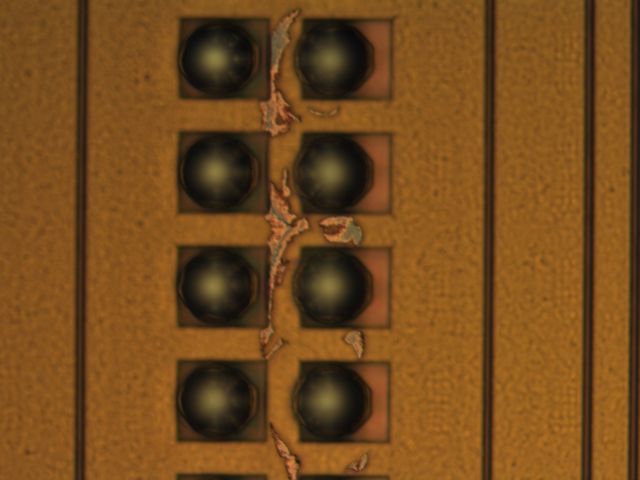
- Bumps x20.jpg: a photo using 20 x magnification:

- Cu and solder x50.jpg: Cu residues after the field metal (Cu) etching.:

- Dummy bumps x5.jpg: This photo is from the wafer perimeter, where the ROCs are not complete.:

| I | Attachment | History | Action | Size | Date | Who | Comment |
|---|---|---|---|---|---|---|---|
| |
10x_-1.jpg | r1 | manage | 70.1 K | 2012-02-22 - 11:14 | RichardBates | 10x -1.jpg: a photo from the chip corner |
| |
Bumps_x20.jpg | r1 | manage | 56.7 K | 2012-02-22 - 11:15 | RichardBates | Bumps x20.jpg: a photo using 20 x magnification |
| |
Cu_and_solder_x50.jpg | r1 | manage | 33.0 K | 2012-02-22 - 11:15 | RichardBates | Cu and solder x50.jpg: Cu residues after the field metal (Cu) etching. |
| |
Dummy_bumps_x5.jpg | r1 | manage | 81.2 K | 2012-02-22 - 11:16 | RichardBates | Dummy bumps x5.jpg: This photo is from the wafer perimeter, where the ROCs are not complete. |
| |
ROW-V6ABC1H-cracked-JS-16-Mar-2012.pdf | r1 | manage | 490.1 K | 2012-04-16 - 14:06 | RichardBates | |
| |
V6ABC1H.ppt | r1 | manage | 557.0 K | 2012-02-22 - 11:11 | RichardBates | Picture of the wafer map |
| |
WafertestingResults_V6ABC1H.xlsx | r1 | manage | 22.5 K | 2012-02-22 - 11:11 | RichardBates | Probe results |
Topic revision: r2 - 2012-04-16 - RichardBates
Ideas, requests, problems regarding TWiki? Send feedback


