The wafer map
- V6ABC1H.ppt: Picture of the wafer map
- WafertestingResults_V6ABC1H.xlsx: Probe results
- 10x -1.jpg: a photo from the chip corner:

- Bumps x20.jpg: a photo using 20 x magnification:

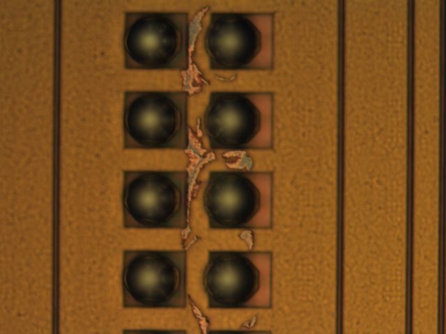
- Cu and solder x50.jpg: Cu residues after the field metal (Cu) etching.:

- Dummy bumps x5.jpg: This photo is from the wafer perimeter, where the ROCs are not complete.:

| I | Attachment | History | Action | Size | Date | Who | Comment |
|---|---|---|---|---|---|---|---|
| |
10x_-1.jpg | r1 | manage | 70.1 K | 2012-02-22 - 11:14 | RichardBates | 10x -1.jpg: a photo from the chip corner |
| |
Bumps_x20.jpg | r1 | manage | 56.7 K | 2012-02-22 - 11:15 | RichardBates | Bumps x20.jpg: a photo using 20 x magnification |
| |
Cu_and_solder_x50.jpg | r1 | manage | 33.0 K | 2012-02-22 - 11:15 | RichardBates | Cu and solder x50.jpg: Cu residues after the field metal (Cu) etching. |
| |
Dummy_bumps_x5.jpg | r1 | manage | 81.2 K | 2012-02-22 - 11:16 | RichardBates | Dummy bumps x5.jpg: This photo is from the wafer perimeter, where the ROCs are not complete. |
| |
V6ABC1H.ppt | r1 | manage | 557.0 K | 2012-02-22 - 11:11 | RichardBates | Picture of the wafer map |
| |
WafertestingResults_V6ABC1H.xlsx | r1 | manage | 22.5 K | 2012-02-22 - 11:11 | RichardBates | Probe results |
Topic revision: r1 - 2012-02-22 - RichardBates
Ideas, requests, problems regarding TWiki? Send feedback


