TWiki
>
DetDev Web
>
TFHybShort
(revision 2) (raw view)
Edit
Attach
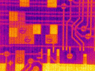
---+++ Introduction Four electrical grade wafers were delivered, plus one that was damaged during fabrication. Each wafer has three hybrids, hence the electrical grade wafers have 12 hybrids and two of the hybrids on the damaged wafer are not affected by the damage. Initial connectivity test with probe needles gave the following results * All 14 hybrids show a short between power and ground, with a resistance dominated by the contact resistance of the needles. * None of the signal lines seem to be shorted to ground (veryfied on one hybrid) * A selection of signal lines were probed on one hybrid, all where connected correctly. ---+++ Thermal imaging, Wafer 08, Hybrid 2 This is the middle hybrid of the damaged wafer. The GND and PWR pads on the power end of the hybrid were connected with 17 bond wires and the voltage difference between the GND and PWR plane was monitoried on the signal end of the hybrid. The V/I characteristics and corresponding resistance are shown below.The graph called Vin is the voltage at the input on the power end, and Vmon is the voltage measured at the signal end. <img width="537" alt="VI_Hyb2_w08.jpg" src="https://ppes8.physics.gla.ac.uk/twiki/pub/DetDev/TFHybShort/VI_Hyb2_w08.jpg" title="VI_Hyb2_w08.jpg" height="310" /><img width="423" alt="Rin_Hyb2_w08.jpg" src="https://ppes8.physics.gla.ac.uk/twiki/pub/DetDev/TFHybShort/Rin_Hyb2_w08.jpg" title="Rin_Hyb2_w08.jpg" height="310" /> The current was scanned many times up to increasing maximum values. Two hot-spots were became visible on the hybrid after a few power cycles. <img width="350" alt="4p5AfromCold_21to32deg_SE_cropped.jpg" src="https://ppes8.physics.gla.ac.uk/twiki/pub/DetDev/TFHybShort/4p5AfromCold_21to32deg_SE_cropped.jpg" title="4p5AfromCold_21to32deg_SE_cropped.jpg" height="214" /> After a few power cycles up to maximums between 5 and 10 A, the the lower hotspot disappeared, but the short remained. <img width="350" alt="10A2862mV_22to60deg_SE_cropped.jpg" src="https://ppes8.physics.gla.ac.uk/twiki/pub/DetDev/TFHybShort/10A2862mV_22to60deg_SE_cropped.jpg" title="10A2862mV_22to60deg_SE_cropped.jpg" height="212" /> These two spots don't correspond to any particular features in the layout. <img width="858" alt="LayoutScreenShot.jpg" src="https://ppes8.physics.gla.ac.uk/twiki/pub/DetDev/TFHybShort/LayoutScreenShot.jpg" title="LayoutScreenShot.jpg" height="377" /> After a further few cycles the short disappeared, and a small crater is visible on the location of the upper hot spot. No damage is visible on the location of the other hot spot. <img width="720" alt="Hyb2_BurntHotspot.jpg" src="https://ppes8.physics.gla.ac.uk/twiki/pub/DetDev/TFHybShort/Hyb2_BurntHotspot.jpg" title="Hyb2_BurntHotspot.jpg" height="576" /> <img width="720" alt="Hyb2_BurntHotspot_close.jpg" src="https://ppes8.physics.gla.ac.uk/twiki/pub/DetDev/TFHybShort/Hyb2_BurntHotspot_close.jpg" title="Hyb2_BurntHotspot_close.jpg" height="576" /> ---+++ Thermal imaging, Wafer 08, Hybrid 1 The same measurements were repeated with hybrid 1 on wafer 8, but this time with a solder connection and only on the power end of the hybrid. The V/I characteristics are shown below. <img width="494" alt="VI_Hyb1_w08.jpg" src="https://ppes8.physics.gla.ac.uk/twiki/pub/DetDev/TFHybShort/VI_Hyb1_w08.jpg" title="VI_Hyb1_w08.jpg" height="328" /><img width="484" alt="Rin_Hyb1_w08.jpg" src="https://ppes8.physics.gla.ac.uk/twiki/pub/DetDev/TFHybShort/Rin_Hyb1_w08.jpg" title="Rin_Hyb1_w08.jpg" height="328" /> The difference in measured resistance (77 vs. 238 mOhm) could be due to the contact resistance. The hybrid was powered repeatedly up to 10 A but no hot spots were visible. All heat dissipation seem to be at the power pads of the hybrids. <img width="320" alt="5A361mV_22to36deg_PE.jpg" src="https://ppes8.physics.gla.ac.uk/twiki/pub/DetDev/TFHybShort/5A361mV_22to36deg_PE.jpg" title="5A361mV_22to36deg_PE.jpg" height="240" /><img width="320" alt="PowerPads_10A.jpg" src="https://ppes8.physics.gla.ac.uk/twiki/pub/DetDev/TFHybShort/PowerPads_10A.jpg" title="PowerPads_10A.jpg" height="240" /> ---+++ Comparison w08, Hybrid 1 & 2 High resolution images of the same location of Hybrid 1 and 2, both with 5 A current. <img width="320" alt="Hotspot1_5A.jpg" src="https://ppes8.physics.gla.ac.uk/twiki/pub/DetDev/TFHybShort/Hotspot1_5A.jpg" title="Hotspot1_5A.jpg" height="240" /><img width="320" alt="SamePosAsHotSpotOnHyb1_5A.jpg" src="https://ppes8.physics.gla.ac.uk/twiki/pub/DetDev/TFHybShort/SamePosAsHotSpotOnHyb1_5A.jpg" title="SamePosAsHotSpotOnHyb1_5A.jpg" height="240" /> ---+++ Thermal imaging, Wafer 01, Hybrid 1 Hybrid 1 on wafer 01 was powered using spring loaded pins on a custom made powering jig. The power supply was in current control mode and the following hotspot was seen at Iin=100 mA and Vin=0.835 V. The pictures show an overview thermal image and a high resolution image of the area, with and without power. <img width="320" alt="100mA835mV_PEsupply_hotspot.jpg" src="https://ppes8.physics.gla.ac.uk/twiki/pub/DetDev/TFHybShort/100mA835mV_PEsupply_hotspot.jpg" title="100mA835mV_PEsupply_hotspot.jpg" height="240" /> <img width="320" alt="100mA835mV_PEsupply_hotspot_highRes.jpg" src="https://ppes8.physics.gla.ac.uk/twiki/pub/DetDev/TFHybShort/100mA835mV_PEsupply_hotspot_highRes.jpg" title="100mA835mV_PEsupply_hotspot_highRes.jpg" height="240" /><img width="320" alt="noPower_PEsupply_hotspot_highRes.jpg" src="https://ppes8.physics.gla.ac.uk/twiki/pub/DetDev/TFHybShort/noPower_PEsupply_hotspot_highRes.jpg" title="noPower_PEsupply_hotspot_highRes.jpg" height="240" /> The short had an approximate resistance of 8 Ohms and almost disappeared at 150 mA current. It was transformed in to a 15 Ohm short that then disappeared at 150 mA. No visible damage is seen in the area (see photo below). The circuit was powered with 35 V between PWR and GND planes for 15 minutes and the measured current was approximately 50 uA. <img width="720" alt="w1h1_hotspot_afterBurn_noDamage.jpg" src="https://ppes8.physics.gla.ac.uk/twiki/pub/DetDev/TFHybShort/w1h1_hotspot_afterBurn_noDamage.jpg" title="w1h1_hotspot_afterBurn_noDamage.jpg" height="576" /> ---+++ Thermal imaging, Wafer 01, Hybrid 2 Hybrid 1 on wafer 01 was powered using spring loaded pins on a custom made powering jig. The power was supplied in current control mode via the power pads in both ends and at 4A and 362 mV the following hotspot was observed. <img width="320" alt="4A362mV_SupplyBothEnds_hotspot.jpg" src="https://ppes8.physics.gla.ac.uk/twiki/pub/DetDev/TFHybShort/4A362mV_SupplyBothEnds_hotspot.jpg" title="4A362mV_SupplyBothEnds_hotspot.jpg" height="240" /> This is a high resolution image of the area at 7A and 680mV and without power <img width="320" alt="7A680mV_SupplyBothEnds_hotspot_highRes.jpg" src="https://ppes8.physics.gla.ac.uk/twiki/pub/DetDev/TFHybShort/7A680mV_SupplyBothEnds_hotspot_highRes.jpg" title="7A680mV_SupplyBothEnds_hotspot_highRes.jpg" height="240" /><img width="320" alt="noPower_SupplyBothEnds_hotspot_highRes.jpg" src="https://ppes8.physics.gla.ac.uk/twiki/pub/DetDev/TFHybShort/noPower_SupplyBothEnds_hotspot_highRes.jpg" title="noPower_SupplyBothEnds_hotspot_highRes.jpg" height="240" /> The short had an approximate resistance of 0.1 Ohm and was burnt away at 9A and 1.04 V. A second short with much higher resistance (approximately12 Ohms) then became visible, here shown at 100mA and 1.17V. <img width="320" alt="100mA1170mV_PEsupply_SE_hotspot.jpg" src="https://ppes8.physics.gla.ac.uk/twiki/pub/DetDev/TFHybShort/100mA1170mV_PEsupply_SE_hotspot.jpg" title="100mA1170mV_PEsupply_SE_hotspot.jpg" height="240" /><img width="320" alt="100mA1170mV_PEsupply_SE_hotspot_highres.jpg" src="https://ppes8.physics.gla.ac.uk/twiki/pub/DetDev/TFHybShort/100mA1170mV_PEsupply_SE_hotspot_highres.jpg" title="100mA1170mV_PEsupply_SE_hotspot_highres.jpg" height="240" /><img width="320" alt="noPower_PEsupply_SE_hotspot_highres.jpg" src="https://ppes8.physics.gla.ac.uk/twiki/pub/DetDev/TFHybShort/noPower_PEsupply_SE_hotspot_highres.jpg" title="noPower_PEsupply_SE_hotspot_highres.jpg" height="240" /> The short disappeard at 250 mA with no visible damage in the area. The hybrid was powered with 35 V between GND and PWR for 15 minutes and the current was approximately 10 uA. ---+++ Wafer 01 Hybrid 3 Hybrid 3 on wafer 1 was powered up to 3 A (Vin = 359 mV @ 3A) without showing any hotspots. Unfortunately the power supply pad burnt out which prevented further investigation of the hybrid. -- Main.LarsEklund - 2010-07-21
Attachments
Attachments
Topic attachments
I
Attachment
History
Action
Size
Date
Who
Comment
jpg
100mA1170mV_PEsupply_SE_hotspot.jpg
r1
manage
13.2 K
2010-08-09 - 20:25
LarsEklund
jpg
100mA1170mV_PEsupply_SE_hotspot_highres.jpg
r1
manage
20.0 K
2010-08-09 - 20:26
LarsEklund
jpg
100mA835mV_PEsupply_hotspot.jpg
r1
manage
10.0 K
2010-08-09 - 20:09
LarsEklund
jpg
100mA835mV_PEsupply_hotspot_highRes.jpg
r1
manage
19.5 K
2010-08-09 - 20:09
LarsEklund
jpg
10A2862mV_22to60deg_SE_cropped.jpg
r1
manage
20.6 K
2010-07-21 - 17:06
LarsEklund
jpg
4A362mV_SupplyBothEnds_hotspot.jpg
r1
manage
14.8 K
2010-08-09 - 20:20
LarsEklund
jpg
4p5AfromCold_21to32deg_SE_cropped.jpg
r1
manage
26.2 K
2010-07-21 - 16:45
LarsEklund
jpg
5A361mV_22to36deg_PE.jpg
r1
manage
12.4 K
2010-07-21 - 17:10
LarsEklund
jpg
7A680mV_SupplyBothEnds_hotspot_highRes.jpg
r1
manage
28.8 K
2010-08-09 - 20:20
LarsEklund
jpg
Hotspot1_5A.jpg
r1
manage
9.8 K
2010-07-21 - 17:15
LarsEklund
jpg
Hyb2_BurntHotspot.jpg
r1
manage
84.1 K
2010-07-21 - 16:58
LarsEklund
jpg
Hyb2_BurntHotspot_close.jpg
r1
manage
62.1 K
2010-07-21 - 16:58
LarsEklund
jpg
LayoutScreenShot.jpg
r1
manage
111.0 K
2010-07-21 - 16:52
LarsEklund
jpg
PowerPads_10A.jpg
r1
manage
11.9 K
2010-07-21 - 17:12
LarsEklund
jpg
Rin_Hyb1_w08.jpg
r1
manage
24.3 K
2010-07-21 - 16:36
LarsEklund
jpg
Rin_Hyb2_w08.jpg
r1
manage
21.7 K
2010-07-21 - 16:36
LarsEklund
jpg
SamePosAsHotSpotOnHyb1_5A.jpg
r1
manage
23.2 K
2010-07-21 - 17:15
LarsEklund
jpg
VI_Hyb1_w08.jpg
r1
manage
24.6 K
2010-07-21 - 16:36
LarsEklund
jpg
VI_Hyb2_w08.jpg
r1
manage
23.9 K
2010-07-21 - 16:36
LarsEklund
jpg
noPower_PEsupply_SE_hotspot_highres.jpg
r1
manage
25.3 K
2010-08-09 - 20:28
LarsEklund
jpg
noPower_PEsupply_hotspot_highRes.jpg
r1
manage
19.5 K
2010-08-09 - 20:10
LarsEklund
jpg
noPower_SupplyBothEnds_hotspot_highRes.jpg
r1
manage
24.7 K
2010-08-09 - 20:20
LarsEklund
jpg
w1h1_hotspot_afterBurn_noDamage.jpg
r1
manage
65.1 K
2010-08-09 - 20:10
LarsEklund
Edit
|
Attach
|
Watch
|
P
rint version
|
H
istory
:
r3
<
r2
<
r1
|
B
acklinks
|
V
iew topic
|
Raw edit
|
More topic actions...
Topic revision: r2 - 2010-08-09
-
LarsEklund
DetDev
Log In
or
Register
DetDev Web
Create New Topic
Index
Search
Changes
Notifications
RSS Feed
Statistics
Preferences
Webs
ATLAS
PUUKA
DetDev
Gridmon
IT
LHCb
LinearCollider
Main
NA62
Sandbox
TWiki
Copyright © 2008-2025 by the contributing authors. All material on this collaboration platform is the property of the contributing authors.
Ideas, requests, problems regarding TWiki?
Send feedback

