Flip-chip bonding at STFC-RAL
STFC/RAL are developing a fine pitched Indium flip-chip process. The samples first have an under bump metal (UBM) layer deposited upon them where the bump is to be grown. The UBM used to date is Ti/W, Ni, Au. The Ti/W is an adhesion layer to the Aluminium pad of the device. The nickel is the solderable metal layer and the Au is an oxidation barrier. The indium is deposited in a thermal reactor at RAL. The Indium is heated under vacuum and condenses on the sample that is held at a lower temperature. The samples can then be flip-chipped bonded. The flip-chip process is to work at room temperature or slightly elevated temperatures.
There is some worry that the Indium bumps require more pressure to form a bump than should be the case. One suggestion for this high pressure is that the gold used in the UBM is moving into the Indium and forming an Indium/Gold alloy which requires more force to deform. A SEM/FIB/EDX study of an Indium bump formed on a silicon substrate was performed in Glasgow to try and test the hypothesis that the gold had moved into the Indium. The report is found here:
- Report_on_SEM_Secondary_electron_images_and_EDX_measurements_on_In_bumps_from_RAL.docx: Report on SEM for Indium bump from RAL
First Indium Flip-chip bonded FE-I4
The first indium assembly wafer ID : VMB6NJH die 3
Sensor : CPII Live FE-I4 MPI Guard IBL
Indium_BumpYield_28032014.pptx: Bump Yield Studies March 2013
Indium Flip-Chipped Modules September 2014
Indium bumps require pressure only to make connections so no high temperatures are required to melt alloy, which reduces bowing effects.
Modules under test:
| ID | Bond Force | Comment |
|---|---|---|
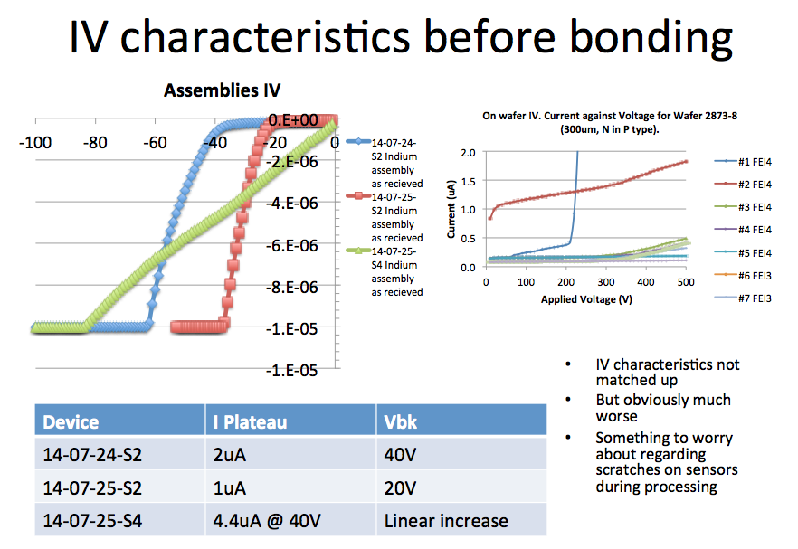
| 14-07-24-S2 | 20kg | biased to 40V |
| 14-07-25-S2 | 10kg | short on VDDA line |
| 14-07-25-S4 | 5kg | biased to 40V (operated at 20V) |
IV Scans
IV Scans on wafer and after processing
Characterisation
USBPix
Bump yield studies performed in August 2014 by Dan Smaranda and Richard Bates
21082014_Indium-DanSmaranda.pdf
RCE System
All modules tuned to and operated at 3000e threshold, 10ToT @ 16ke reference charge.
Tuning
Module 14-07-24_S2:
Tune to 3000e, 10ToT @ 16ke
Module 14-07-25_S4:
Tune to 3000e, 10ToT @ 16ke
Bump Yield Studies
Bump Yield assessed by performing Threshold Scans with and without sensor bias and performing source scans with Strontium-90 beta source and Americium-241 60keV gamma ray source.
Indium-Characterisation_0914.pptx
Bump yield results
| Module | Bond Force | Bump Yield (Sigma plot) |
Bump Yield (Source Scans) |
|---|---|---|---|
| 14-07-25-S4 | 5kg | 23.37% | 22.54% |
| 14-07-24-S2 | 20kg | 82.85% | 82.35% |
| Indium1 | ? | 99.48% | 99.38% |
Comments
|
|
Ideas, requests, problems regarding TWiki? Send feedback