Wafer and sensor numbering scheme
The wafers are marked with sensor number at the wafer edge close to the larger straight section of the border. The individual sensors are labelled by their X and Y positions on the wafer. The classification of the wafers and the definition of the wafer number can be found in SensorNumbering.pdf.
Electrical measurements of Run 1
I/V and C/V measurements of all sensors before dicingDocumentation and photos
Photos at reception of the wafers Bias bonds on measured wafers Yield measurementsMechanical measurements
Sensor flatness Photos at reception of Run 1 wafers The photos were taken at reception of the wafers, but after wafers w09 and w14 had some of their ground planes bonded to the bias rails. Bond tests and tuning were done on the large metallised area at the bottom of w09. The bonds are visible in the photos. The bias bond locations are described in BiasBonds.pdf. Full wafer views| 6 um BCB | 12 um BCB | |
| Electrical | w14, w15 | w08, w09 |
| Mechanical | w17, w18, w19 | w04, w05, w16 |
IV and CV measurments
Measurements performed by Alex Chilingarov, University of Lancaster and analysis is done by Lars Eklund, University of Glasgow.Summary plots of I/V and C/V performance for wafer 09 (12 µm BCB)
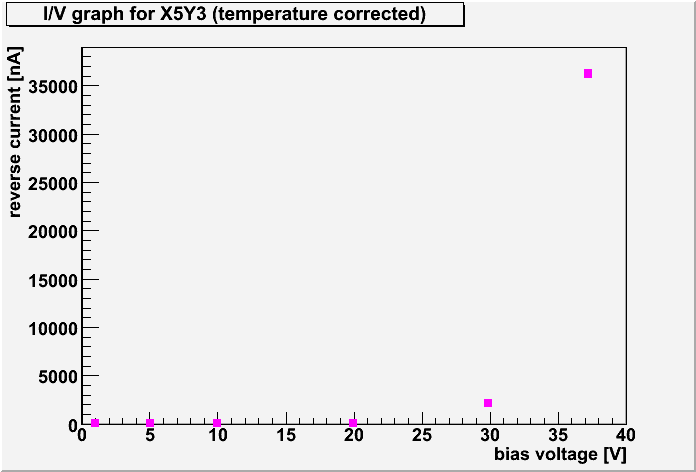
The scale of the I/V graph covers the range of 25 of the 26 sensors on wafer 09. Sensor X5Y3 breakes down at low voltages, see separate I/V. Sensors X5Y1, X5Y2 and X5Y4 were ramped to 600 V with leakage current of 40, 33 and 31 nA at 600V. Sensor X5Y1 was kept at 600 V for 30 min and is the only sensor that shows a clear change in reverse current over time, but with signs of saturation. See stability graph.


 Depletion voltage extracted from C/V
The depletion voltage was extracted by fitting two first order polynomials to the 1/C2 vs. Vbias graph. The first straight line is fitted between 0 and 30 V and the second straight line is fitted between 150 and 400 V. The depletion voltage is defined as the intersection between these two lines. The depletion voltage is displayed both as a histogram and as a map where the depletion voltage is displayed in its position on the wafer, with coordinates as defined in the figure above. The depletion voltage could not be determined for X5Y3 due to its breakdown, hence the histograms include 25 sensors.
Depletion voltage extracted from C/V
The depletion voltage was extracted by fitting two first order polynomials to the 1/C2 vs. Vbias graph. The first straight line is fitted between 0 and 30 V and the second straight line is fitted between 150 and 400 V. The depletion voltage is defined as the intersection between these two lines. The depletion voltage is displayed both as a histogram and as a map where the depletion voltage is displayed in its position on the wafer, with coordinates as defined in the figure above. The depletion voltage could not be determined for X5Y3 due to its breakdown, hence the histograms include 25 sensors.


Summary plots of I/V and C/V performance for wafer 14 (6 µm BCB)
Until present 19 sensors have been teste of which 18 are inclueded in the plots. Sensor X0Y4 broke down a very low voltage and is excluded from the analysis presented here.


 Depletion voltage extracted from C/V
The depletion voltage was extracted by fitting two first order polynomials to the 1/C2 vs. Vbias graph. The first straight line is fitted between 0 and 30 V and the second straight line is fitted between 150 and 400 V. The depletion voltage is defined as the intersection between these two lines. The depletion voltage is displayed both as a histogram and as a map where the depletion voltage is displayed in its position on the wafer, with coordinates as defined in the figure above. Sensor X0Y4 is not inclued in the depletion voltage plots since it broke down at low voltages.
Depletion voltage extracted from C/V
The depletion voltage was extracted by fitting two first order polynomials to the 1/C2 vs. Vbias graph. The first straight line is fitted between 0 and 30 V and the second straight line is fitted between 150 and 400 V. The depletion voltage is defined as the intersection between these two lines. The depletion voltage is displayed both as a histogram and as a map where the depletion voltage is displayed in its position on the wafer, with coordinates as defined in the figure above. Sensor X0Y4 is not inclued in the depletion voltage plots since it broke down at low voltages.


 Sensor X5Y1 was kept at 1000V and a break down started to develop at which point it was ramped down immediately

Plots combining the I/V and C/V data for wafer 09 and 14
 The following plot show the reverse current at 400 V bias for all measured sensors on wafer 09 and 14.
 The following plot shows the reverse current at 400 and 600 V for w 14 for all measured sensors
 -- LarsEklund - 21 Nov 2008

Topic revision: r17 - 2008-12-16 - LarsEklund
|
|
Ideas, requests, problems regarding TWiki? Send feedback