TWiki
>
DetDev Web
>
MCMD
(revision 13) (raw view)
Edit
Attach
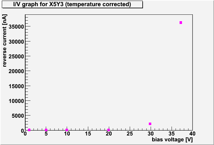
---+++ Wafer and sensor numbering scheme The wafers are marked with sensor number at the wafer edge close to the larger straight section of the border. The individual sensors are labelled by their X and Y positions on the wafer. The classification of the wafers and the definition of the wafer number can be found in [[%ATTACHURL%/SensorNumbering.pdf][SensorNumbering.pdf]]. <img width="422" alt="Sensor number scheme" src="%ATTACHURL%/sensorOverviewNumbered.jpg" height="400" /> ---+++ Photos at reception of Run 1 wafers The photos were taken at reception of the wafers, but after wafers w09 and w14 had some of their ground planes bonded to the bias rails. Bond tests and tuning were done on the large metallised area at the bottom of w09. The bonds are visible in the photos. The bias bond locations are described in [[%ATTACHURL%/BiasBonds.pdf][BiasBonds.pdf.]] *Full wafer views* | | 6 um BCB | 12 um BCB | | Electrical | [[%ATTACHURL%/w14_6umBCBElectrical_atReception.JPG][w14]], [[%ATTACHURL%/w15_6umBCBElectrical_atReception.JPG][w15]] | [[%ATTACHURL%/w08_12umBCBElectrical_atReception.JPG][w08]], [[%ATTACHURL%/w09_12umBCBElectrical_atReception.JPG][w09]] | | Mechanical | [[%ATTACHURL%/w17_6umBCBMechanical_atReception.JPG][w17]], [[%ATTACHURL%/w18_6umBCBMechanical_atReception.JPG][w18]], [[%ATTACHURL%/w19_6umBCBMechanical_atReception.JPG][w19]] | [[%ATTACHURL%/w04_12umBCBMechanical_atReception.JPG][w04]], [[%ATTACHURL%/w05_12umBCBMechanical_atReception.JPG][w05]], [[%ATTACHURL%/w16_12umBCBMechanical_atReception.JPG][w16]] | *Close-up views on a few sensors on w14* [[%ATTACHURL%/meshGNDPlane_w14_X3Y2.JPG][Meshed GND plane, full view]] [[%ATTACHURL%/meshGNDPlane_w14_X0Y1.JPG][Bias bond, close-up]] [[%ATTACHURL%/meshGNDPlane_w14_X4Y1.JPG][Meshed GND plane, top half]] [[%ATTACHURL%/meshGNDPlane_w14_X4Y2.JPG][Meshed GND plane, full view]] [[%ATTACHURL%/solidGNDPlane_w14_X3Y1.JPG][Solid GND plane, top half]] [[%ATTACHURL%/triGNDPlane_w14_X3Y0.JPG][Triangular GND plane, full view]] *Close-up views on a few features on w14* Ground planes: [[%ATTACHURL%/solidGNDPlane.jpg][solid]], [[%ATTACHURL%/meshedGNDPlane.jpg][meshed]], [[%ATTACHURL%/meshedGNDPlane_withBondPad2.jpg][meshed (bond pad)]] Bias and guard ring connections: [[%ATTACHURL%/biasGuardRings.jpg][bias and guard rings]], [[%ATTACHURL%/biasRingVia_zoom.JPG][bias ring via]], [[%ATTACHURL%/biasBonds_tri.jpg][bias bond (triangular)]], [[%ATTACHURL%/meshedGNDPlane_withBondPad.jpg][bias bond (meshed)]] Strip connections: [[%ATTACHURL%/stripPadConnections.jpg][overview]], [[%ATTACHURL%/stripPadConnections_zoom1.jpg][zoom 1]], [[%ATTACHURL%/stripPadConnections_zoom2.jpg][zoom 2]], [[%ATTACHURL%/stripPadConnections_zoom3.jpg][zoom 3]], [[%ATTACHURL%/bondPad.jpg][bond pad]], [[%ATTACHURL%/doubleVias.jpg][double vias]] Bias resistor connections: [[%ATTACHURL%/biasResVias.jpg][resistor via]], [[%ATTACHURL%/biasResVia_zoom.jpg][zoom]] A set of lines with decreasing line width and spacing were put on the mask to assess the resolution of the process. Starting with 10 lines of 5 um line width and spacing, increasing with 5 um for each set of lines. As seen in the [[%ATTACHURL%/lineResolution.jpg][overview picture]] all lines down to 10 um line width and spacing were correctly reproduced. However, the smallest pitch region became merged into one solid metallisation as can be seen in the [[%ATTACHURL%/lineResolution_zoom.jpg][close-up]]. ---+++ IV and CV measurments Measurements performed by Alex Chilingarov, University of Lancaster and analysis is done by Lars Eklund, University of Glasgow. ---++++ *Summary plots of I/V and C/V performance for wafer 09 (12 µm BCB)* The scale of the I/V graph covers the range of 25 of the 26 sensors on wafer 09. Sensor X5Y3 brakes down at low voltages, see [[%ATTACHURL%/X5Y3_IVgraph.gif][separate I/V]]. Sensors X5Y1, X5Y2 and X5Y4 were ramped to 600 V with leakage current of 40, 33 and 31 nA at 600V. Sensor X5Y1 was kept at 600 V for 30 min and is the only sensor that shows a clear change in reverse current over time, but with signs of saturation. See [[%ATTACHURL%/X5Y1_biasStability.gif][stability graph]]. <img width="596" alt="I/V characteristics of all sensors" src="%ATTACHURL%/w09_IVSummary.gif" height="372" /> <img width="596" alt="Summary of all C/V on wafer 09" src="%ATTACHURL%/w09_CVSummary.gif" height="372" /> <img width="596" alt="1/C² vs V graphs for all sensors on w09" src="%ATTACHURL%/w09_1_C2vsV_Summary.gif" height="372" /> <img width="596" alt="Rs vs V summary graph" src="%ATTACHURL%/w09_RsVSummary.gif" height="372" /> <img width="596" alt="" src="%ATTACHURL%/w09I400Map.gif" height="372" /> *Depletion voltage extracted from C/V* The depletion voltage was extracted by fitting two first order polynomials to the 1/C2 vs. Vbias graph. The first straight line is fitted between 0 and 30 V and the second straight line is fitted between 150 and 400 V. The depletion voltage is defined as the intersection between these two lines. The depletion voltage is displayed both as a histogram and as a map where the depletion voltage is displayed in its position on the wafer, with coordinates as defined in the figure above. The depletion voltage could not be determined for X5Y3 due to its breakdown, hence the histograms include 25 sensors. <img width="596" alt="Wafer map of depletion voltages" src="%ATTACHURL%/w09_VdepMap.gif" height="372" /> <img width="596" alt="Histogram of measured depletion voltages" src="%ATTACHURL%/w09_VdepHisto.gif" height="372" /> ---++++ ---++++ *Summary plots of I/V and C/V performance for wafer 14 (6 µm BCB)* Until present 19 sensors have been teste of which 18 are inclueded in the plots. Sensor X0Y4 broke down a very low voltage and is excluded from the analysis presented here. <img width="596" alt="I/V characteristics of all sensors" src="%ATTACHURL%/w14_IVSummary.gif" height="372" /> <img width="596" alt="Summary of all C/V on wafer 09" src="%ATTACHURL%/w14_CVSummary.gif" height="372" /> <img alt="1/C² vs V graphs for all sensors on w09" src="%ATTACHURL%/w14_1_C2vsV_Summary.gif" /> <img width="596" alt="Rs vs V summary graph" src="%ATTACHURL%/w14_RsVSummary.gif" height="372" /> <img width="596" alt="" src="%ATTACHURL%/w14I400Map.gif" height="372" /> <img width="596" alt="" src="%ATTACHURL%/w14I600Map.gif" height="372" /> *Depletion voltage extracted from C/V* The depletion voltage was extracted by fitting two first order polynomials to the 1/C2 vs. Vbias graph. The first straight line is fitted between 0 and 30 V and the second straight line is fitted between 150 and 400 V. The depletion voltage is defined as the intersection between these two lines. The depletion voltage is displayed both as a histogram and as a map where the depletion voltage is displayed in its position on the wafer, with coordinates as defined in the figure above. Sensor X0Y4 is not inclued in the depletion voltage plots since it broke down at low voltages. <img width="596" alt="Wafer map of depletion voltages" src="%ATTACHURL%/w14_VdepMap.gif" height="372" /> ---++++ <img width="596" alt="Histogram of measured depletion voltages" src="%ATTACHURL%/w14_VdepHisto.gif" height="372" /> ---++++ Plots combining the I/V and C/V data for wafer 09 and 14 <img width="596" alt="Combined depletion voltages for wafer 09 nad 14" src="%ATTACHURL%/combined_Vdepl.gif" height="372" /> The following plot show the reverse current at 400 V bias for all measured sensors on wafer 09 and 14. <img width="596" alt="current at 400 V for all sensors on w 09 and w 14" src="%ATTACHURL%/combined_I400.gif" height="372" /> The following plot shows the reverse current at 400 and 600 V for w 14 for all measured sensors <img width="596" alt="Current at 400 and 600 V for w14" src="%ATTACHURL%/combined_Iw14.gif" height="372" /> -- Main.LarsEklund - 21 Nov 2008
Attachments
Attachments
Topic attachments
I
Attachment
History
Action
Size
Date
Who
Comment
pdf
BiasBonds.pdf
r1
manage
628.6 K
2008-11-21 - 15:28
LarsEklund
pdf
SensorNumbering.pdf
r1
manage
346.5 K
2008-11-21 - 15:23
LarsEklund
gif
X5Y1_biasStability.gif
r1
manage
11.2 K
2008-12-08 - 11:22
LarsEklund
gif
X5Y3_IVgraph.gif
r1
manage
7.6 K
2008-12-08 - 10:35
LarsEklund
jpg
biasBonds_mesh.jpg
r1
manage
1939.0 K
2008-11-21 - 18:14
LarsEklund
jpg
biasBonds_tri.jpg
r1
manage
1769.3 K
2008-11-21 - 18:14
LarsEklund
jpg
biasGuardRings.jpg
r1
manage
1950.0 K
2008-11-21 - 18:14
LarsEklund
jpg
biasResVia_zoom.jpg
r1
manage
2221.3 K
2008-11-21 - 18:42
LarsEklund
jpg
biasResVias.jpg
r1
manage
1901.1 K
2008-11-21 - 18:15
LarsEklund
jpg
biasRingVia_zoom.JPG
r1
manage
1967.0 K
2008-11-21 - 18:43
LarsEklund
jpg
bondPad.jpg
r1
manage
1897.3 K
2008-11-21 - 18:16
LarsEklund
gif
combined_I400.gif
r2
r1
manage
8.6 K
2008-12-10 - 23:20
LarsEklund
gif
combined_Iw14.gif
r1
manage
9.5 K
2008-12-10 - 23:22
LarsEklund
gif
combined_Vdepl.gif
r4
r3
r2
r1
manage
6.9 K
2008-12-11 - 11:18
LarsEklund
jpg
doubleVias.jpg
r1
manage
1873.4 K
2008-11-21 - 18:16
LarsEklund
jpg
lineResolution.jpg
r1
manage
2707.7 K
2008-11-21 - 18:16
LarsEklund
jpg
lineResolution_zoom.jpg
r1
manage
2238.2 K
2008-11-21 - 18:16
LarsEklund
jpg
meshGNDPlane_w14_X0Y1.JPG
r1
manage
1523.3 K
2008-11-21 - 15:31
LarsEklund
jpg
meshGNDPlane_w14_X3Y2.JPG
r1
manage
2120.5 K
2008-11-21 - 15:31
LarsEklund
jpg
meshGNDPlane_w14_X4Y1.JPG
r1
manage
1977.7 K
2008-11-21 - 15:32
LarsEklund
jpg
meshGNDPlane_w14_X4Y2.JPG
r1
manage
1307.7 K
2008-11-21 - 15:32
LarsEklund
jpg
meshedGNDPlane.jpg
r1
manage
1771.8 K
2008-11-21 - 18:17
LarsEklund
jpg
meshedGNDPlane_withBondPad.jpg
r1
manage
1755.0 K
2008-11-21 - 18:17
LarsEklund
jpg
meshedGNDPlane_withBondPad2.jpg
r1
manage
1874.4 K
2008-11-21 - 18:17
LarsEklund
jpg
sensorOverviewNumbered.jpg
r1
manage
178.0 K
2008-11-21 - 15:25
LarsEklund
jpg
solidGNDPlane.jpg
r1
manage
1707.4 K
2008-11-21 - 18:17
LarsEklund
jpg
solidGNDPlane_w14_X3Y1.JPG
r1
manage
2101.8 K
2008-11-21 - 15:43
LarsEklund
jpg
stripPadConnections.jpg
r1
manage
2016.9 K
2008-11-21 - 18:18
LarsEklund
jpg
stripPadConnections_zoom1.jpg
r1
manage
1871.6 K
2008-11-21 - 18:18
LarsEklund
jpg
stripPadConnections_zoom2.jpg
r1
manage
1982.4 K
2008-11-21 - 18:18
LarsEklund
jpg
stripPadConnections_zoom3.jpg
r1
manage
2468.9 K
2008-11-21 - 18:18
LarsEklund
jpg
triGNDPlane_w14_X3Y0.JPG
r1
manage
2165.5 K
2008-11-21 - 15:43
LarsEklund
jpg
w04_12umBCBMechanical_atReception.JPG
r1
manage
2386.5 K
2008-11-21 - 12:21
LarsEklund
jpg
w05_12umBCBMechanical_atReception.JPG
r1
manage
2448.2 K
2008-11-21 - 12:21
LarsEklund
jpg
w08_12umBCBElectrical_atReception.JPG
r1
manage
2381.8 K
2008-11-21 - 12:24
LarsEklund
gif
w09I400Map.gif
r2
r1
manage
12.1 K
2008-12-11 - 11:19
LarsEklund
jpg
w09_12umBCBElectrical_atReception.JPG
r1
manage
2381.0 K
2008-11-21 - 12:24
LarsEklund
gif
w09_1_C2vsV_Summary.gif
r7
r6
r5
r4
r3
manage
11.8 K
2008-12-10 - 22:48
LarsEklund
gif
w09_CVSummary.gif
r8
r7
r6
r5
r4
manage
10.3 K
2008-12-10 - 22:49
LarsEklund
gif
w09_IVSummary.gif
r11
r10
r9
r8
r7
manage
15.5 K
2008-12-11 - 10:05
LarsEklund
gif
w09_RsVSummary.gif
r7
r6
r5
r4
r3
manage
15.5 K
2008-12-10 - 22:49
LarsEklund
gif
w09_VdepHisto.gif
r8
r7
r6
r5
r4
manage
6.4 K
2008-12-11 - 11:23
LarsEklund
gif
w09_VdepMap.gif
r5
r4
r3
r2
r1
manage
13.3 K
2008-12-10 - 22:50
LarsEklund
gif
w14I400Map.gif
r2
r1
manage
11.8 K
2008-12-11 - 11:19
LarsEklund
gif
w14I600Map.gif
r2
r1
manage
13.1 K
2008-12-11 - 11:20
LarsEklund
gif
w14_1_C2vsV_Summary.gif
r3
r2
r1
manage
11.1 K
2008-12-10 - 22:50
LarsEklund
jpg
w14_6umBCBElectrical_atReception.JPG
r1
manage
2357.0 K
2008-11-21 - 12:24
LarsEklund
gif
w14_CVSummary.gif
r3
r2
r1
manage
10.0 K
2008-12-10 - 22:50
LarsEklund
gif
w14_IVSummary.gif
r2
r1
manage
15.1 K
2008-12-09 - 18:45
LarsEklund
gif
w14_RsVSummary.gif
r3
r2
r1
manage
18.7 K
2008-12-10 - 22:51
LarsEklund
gif
w14_VdepHisto.gif
r3
r2
r1
manage
6.4 K
2008-12-10 - 22:51
LarsEklund
gif
w14_VdepMap.gif
r3
r2
r1
manage
13.2 K
2008-12-10 - 22:52
LarsEklund
jpg
w15_6umBCBElectrical_atReception.JPG
r1
manage
2338.5 K
2008-11-21 - 12:24
LarsEklund
jpg
w16_12umBCBMechanical_atReception.JPG
r1
manage
2331.5 K
2008-11-21 - 12:24
LarsEklund
jpg
w17_6umBCBMechanical_atReception.JPG
r1
manage
2367.5 K
2008-11-21 - 12:25
LarsEklund
jpg
w18_6umBCBMechanical_atReception.JPG
r1
manage
2350.4 K
2008-11-21 - 12:25
LarsEklund
jpg
w19_6umBCBMechanical_atReception.JPG
r1
manage
2412.7 K
2008-11-21 - 12:25
LarsEklund
Edit
|
Attach
|
Watch
|
P
rint version
|
H
istory
:
r33
|
r15
<
r14
<
r13
<
r12
|
B
acklinks
|
V
iew topic
|
Raw edit
|
More topic actions...
Topic revision: r13 - 2008-12-11
-
LarsEklund
DetDev
Log In
or
Register
DetDev Web
Create New Topic
Index
Search
Changes
Notifications
RSS Feed
Statistics
Preferences
Webs
ATLAS
PUUKA
DetDev
Gridmon
IT
LHCb
LinearCollider
Main
NA62
Sandbox
TWiki
Copyright © 2008-2025 by the contributing authors. All material on this collaboration platform is the property of the contributing authors.
Ideas, requests, problems regarding TWiki?
Send feedback

